OK, so you want to build your own? No problem. I however should mention before you start (even just buying some parts), that there is no warranty at all. No warranty it will be working, no warranty, it will be beautiful, no warranty it won't break your precious rig. No, nothing... All information given here is presented as is. If you'll find any errors, I'll be happy correcting them. But other than that, you're on your own...
Download schematic and pcb from the pages before. To get the parts: For European hams there exists a complete all-in-one parts-list for www.reichelt.de, which you can use to get every single required part including the Fischer aluminium-housing KOH-100. If you follow this link, you'll see the list:
https://secure.reichelt.de/index.html?&ACTION=20&LA=5010&AWKID=1159985&PROVID=2084
This even is useful if you do not want to order your parts directly via Reichelt but via some other distributor as you can see the manufacturer of the parts and the manufacturers item-numbers. This should make it quite easy to get all the parts from somewhere else.
The schematic only shows a very few and easy parts. So, most probably it's not a big risk of just throwing all parts onto the board quickly soldering them all at once and be done with it. If you, however would like to avoid nasty debugging and if this project is maybe your first DIY-project, then it might be advisable to go for the little slower but much less error-prone way of building the keyer step-by-step:
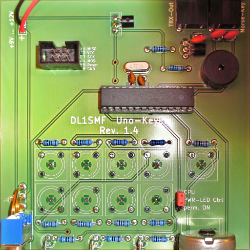
At first solder in the switch SW1, the battery-clip-cable BT1, the two electrolytic capacitors C4 and C5 (both 100µF) and the linear regulator 78L05 U1. Additionally solder R12 (680 Ohm), the power-LED (green, 3.2mcd, low-current) and the three-pins-header J1. Put a short-circuit-jumper on J1 so, that PWR-LED-Ctrl is set to permanent ON. Double check the polarity of each component before you solder them (Remember: the best way of unsoldering parts is NOT to solder them in the wrong way... ;-) )
Now you can attach a 9V battery, and verify that the power-supply for the keyer-board is working like intended. Please check that the switch is working, that the middle pin of J1 has 5.0 Volts against GND (or the - pole of the battery). In that configuration it would be a good idea to see the LED lit when the switch is turned on and the Jumper J1 is set appropriately...
Now solder R1, C1, C2, C3, C6 and C7 as well as the 16MHz crystal. Also do add the speaker, the pin-header for the ICSP-Interface (double check, that the notch is at the correct position!) and the DIL-28 socket for the Atmega 328. Double-ReCheck everything, place Atmega into the socket and don't turn it on. If you do nothing should happen either as it doesn't have a firmware on it, now...
Plug in your favorite ICSP-Adapter (I like USB-ASP, btw... -- only a few bucks on ebay...), fire up the Arduino-IDE, open the keyer-project of which you want to burn the resulting firmware on the µC and burn a regular Arduino UNO Bootloader, first (this is just done, so you don't have to fiddle with the fuse-bits). After that use "Sketch->Upload with programmer" to upload the firmware.
After the upload has successfully been done, the µC board will be reset by the programmer. You should hear a friendly "bleep-up" out of the speaker and if J1 is set to CPU-controlled power-LED, it should be lit, now, too (and start to blink after some time). If all this happens: Lucky you! ;-) the keyer while still lacking some control-elements is working.
The only missing components are the buttons (SW2...SW10), their resistors (R2...R10), the speed-potentiometer (RV1), the control-LED, the TX-LED and the respective LED-resistors (R13, R14). All these components are totally uncritical. Despite two little oddities:
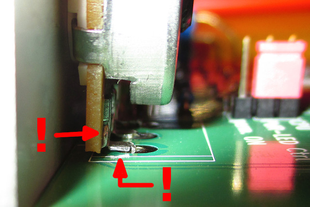
As can be seen in the above image, the buttons must be placed on the other side of the board. If you don't do this you will have a very daunting job of getting these out of the PCB again, clean them and finally place them on the other side of the board as shown in the above image. If placed on this side of the PCB, then the buttons won't come through the top-cover of the housing and the keyer will remain unusable if placed into a nice box...
If you mount the potentiometer RV1 for the WPM-speed you must bend the pins like shown in the image above. If properly bent, the pins have a "double-L" shape. This will serve two purposes: 1. It reduces the height of the potentiometer above the PCB and will allow for a snuggly fit into the housing. Unbent it will not fit into the housing. 2. It will make the potentiometer be better aligned with the front-panel of the box.
It is advisable to test the potentiometer with the bent pins before soldering it onto the board. Getting this beast out again without killing the PCB is a really silly job... Unfortunately I know what I am talking about, here...
Now solder the left components: The mini-jacks used for morse-key and TRX-connection, Blocking-capacitors C8, C9, C10, the switching Transistor Q1 (BC-547C or similar) and it's according resistor R11.
- Obtaining the parts, the pcb and the housing
- Soldering and testing
- Flashing the firmware
- Soldering the still missing components
OK, now you should have a working keyer. If not, please double and tripple check the schematic against your build. If this really doesn't help in making it running, drop me a note to dl1smf@darc.de.